LTspice Mac版で、ロジック・ゲートを使用したデジタル・シミュレーションを行う方法を解説します。
ロジック・シンボルの種類
LTspiceには、次表に示す16種類のロジック・ゲートのシンボルが用意されています。
| Symbol | Description |
|---|---|
| and | Behavioral AND gate |
| buf | Behavioral buffer with complementary outputs |
| buf1 | Behavioral buffer |
| counter | Behavioral counter |
| dflop | Behavioral D-flipflop |
| diffschmitt | Behavioral Schmitt-Triggered Buffer with Complementary Output and Differential Input |
| diffschmtbuf | Behavioral Schmitt-Triggered Buffer with Differential Input |
| diffschmtinv | Behavioral Schmitt-Triggered inverter with Differential Input |
| inv | Behavioral Inverter |
| or | Behavioral OR gate with Complementary Outputs |
| phidet | Behavioral Type 3/4 Phase Detector (Phase/Frequency Detector). Note: Limit input rise times |
| schmitt | Behavioral Schmitt-Triggered buffer with complementary outputs |
| schmtbuf | Behavioral Schmitt-Triggered buffer |
| shmitinv | Behavioral Schmitt-Triggered inverter |
| srflop | Behavioral Set-Reset Flipflop |
| xor | Behavioral XOR gate |
これだけあれば、小規模のデジタル回路ならば容易に対応できます。
ロジック・シンボルのパラメータ
ロジック・ゲートのシンボルには、基本的に以下のパラメータが用意されています。
| Parameter | Default Value | Description |
|---|---|---|
| Vhign | 1 | Logic high level |
| Vlow | 0 | Logic low level |
| Trise | 0 | Rise time |
| Tfall | Trise | Fall time |
| Tau | 0 | Output EC time constant |
| Cout | 0 | Output capatitance |
| Rout | 1 | Output impedance |
| Rhigh | Rout | Logic high level impeance |
| Rlow | Rout | Logic low level impedancde |
| Td | 0 | Propagation delay |
| Ref | 0.5*(Vhigh+Vlow) | Input Logic threshold |
| Vt | 0.5*(Vhigh+Vlow) | Schmitt Input trip point |
| Vh | 0.1 | Schmitt Input hysteresis(one side) |
Trise、Tfall、Td等の遅延タイミングに関するものや、Vt等のロジック入力のレベル判定閾値に関するパラメータの設定が可能です。
ロジックシンボルの応用例
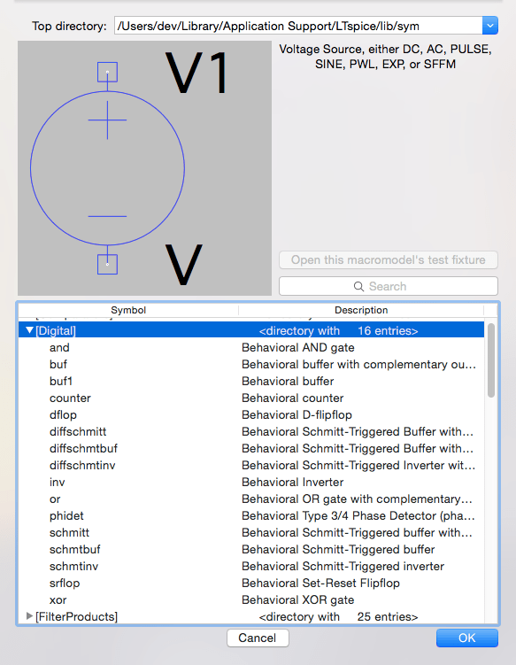
上記のロジック・ゲートを用いてシミュレーション解析を行ってみましょう。回路図で右クリック→Draft→Componentを選択して部品選択のメニューを表示させます。Select Component Symbolの[Digital]を選択します。
(Rignt Click→Draft→Component: Digital)

ロジック・ゲートのシンボル一覧が表示されます。
(Digital Components)
通常の素子と同じ様に回路を作成します。
(Example)

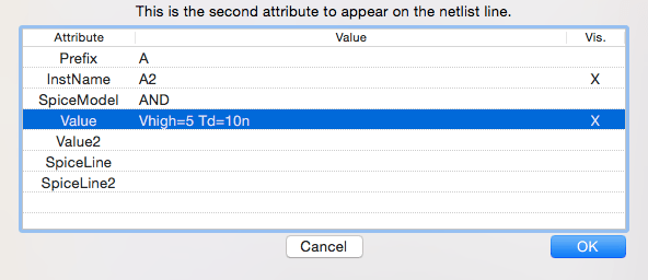
シンボルを右クリックするとAttribute Editorが表示されるので、パラメータの設定を記述します。ここでは、Vhigh=5、Td=5nに設定しています。
(A1 Settings)

Vis.にチェックを入れれば、回路図上にパラメータが表示されます。
(A2 Settings)
シミュレーションに使用する回路を完成させ、シミュレーション解析を実行します。
(Simulation Results)

通常の回路と同じ様に、シミュレーションの結果を確認する事ができます。
COM端子と入力信号の処理
ロジック・ゲートを使用したシミュレーション回路では、COM端子と未使用の入力端子の処理に注意が必要です。以下に処理方法をまとめておきます。
COM端子の位置
4入力以下のシンボル:左下角に配置された端子。
5入力のシンボル:左下角の入力端子の直ぐ右隣に配置された端子。
COM端子の処理
通常GNDに接続しておきます。
不使用の入力端子の処理
通常COM端子に接続しておきます。
注意事項
入力端子をCOM(GND)に接続しても、入力の論理レベルが”L”と解釈される訳ではありません。入力を”L”にしたい場合は、別途用意したVt以下の電圧ノード(例えば0V設定の電源)に接続する必要があるので、注意しましょう。
→その他のLTspice関連情報
Sponsored Link